+86 13638632902
 Jason@cleanroomequips.com
 MENU
MENUX
This project involves the construction of a new Class 100 cleanroom enclosure for wet cleaning processes at Jingxin Semiconductor's Huangshi facility. It is primarily designed to support various wet cleaning, surface treatment, and related front-end process stages involved in the production of 8-inch and 12-inch semiconductor wafers. Designed and constructed with the core objectives of "high cleanliness, high stability, and high reliability" in mind, the project incorporates Modular Air Handling Units (MAU+FFU), a three-stage filtration system (primary, secondary, and HEPA), an optimized air supply and return layout, and a precision temperature and humidity control system. Its primary focus is to effectively address the critical sensitivity of the cleaning zones to contaminants—such as particulates, metal ions, and organic residues—thereby providing a stable and reliable process environment for subsequent key operations, including photolithography and thin-film deposition.
Jingxin Semiconductor is a high-tech enterprise specializing in the manufacturing of integrated circuit chips and power devices. With multiple production and R&D bases established across China, the company’s product portfolio spans a wide range of application sectors, including consumer electronics, industrial control, and new energy vehicles. The company possesses a mature wafer fabrication process platform and a comprehensive quality management system (certified under standards such as ISO 9001 and ISO 14001), maintaining rigorous standards for cleanroom environments and process stability. The recent addition of a Class 1000 cleanroom for cleaning processes at its Huangshi facility represents a pivotal step within the company's strategic framework for expanding production capacity and enhancing manufacturing yield rates.
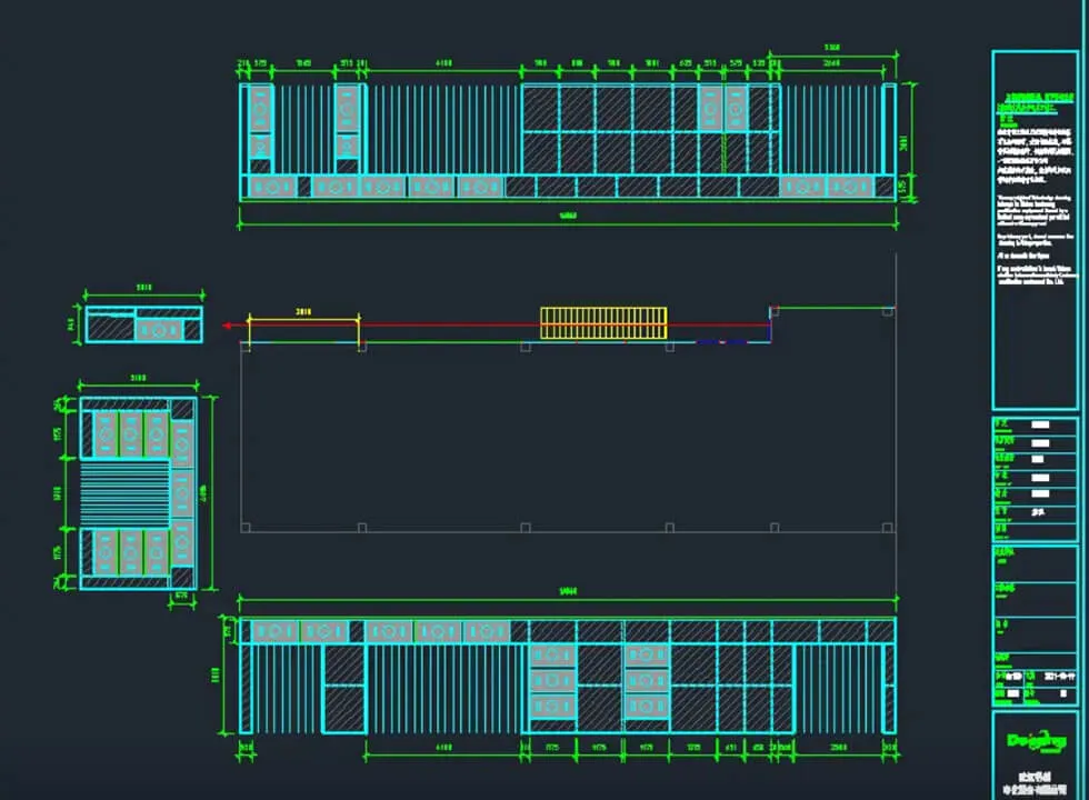
As a vital component of Jingxin Semiconductor’s 12-inch wafer reclamation project, this cleanroom facility commenced construction in the fourth quarter of 2024, with the completion of structural work and system commissioning taking approximately four months. Situated within the main manufacturing plant of the Huangshi Economic and Technological Development Zone, the project fully leverages existing facility space through renovation and upgrading. Adhering strictly to semiconductor industry cleanroom design standards—and taking into account the high sensitivity of the cleaning processes to their micro-environment—the project adopts a design philosophy characterized by "gradient control and localized enhancement." The core cleaning zone is constructed to ISO Class 6 (Class 1,000) standards; furthermore, for critical workstations such as final wafer cleaning, the installation of additional FFUs (Fan Filter Units) enables localized ISO Class 5 (Class 100) control, thereby ensuring that the air cleanliness within critical exposure zones fully meets process requirements.
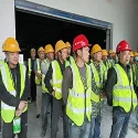
This project is entrusted to our experienced cleanroom construction team, which consists of 5 project managers, 15 engineers, and 40 skilled technicians. All team members hold relevant professional certifications and have undergone specialized training in cleanroom construction, thereby ensuring the project's high quality and timely completion.
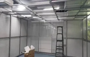
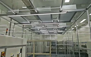
The construction phase best demonstrates Deyiang's team strength and engineering excellence.
Due to the clean booth being located within an existing workshop with complex environmental airflow patterns, we utilized CFD (Computational Fluid Dynamics) airflow simulation to precisely plan and arrange the layout of FFU (Fan Filter Unit) arrays, ensuring optimal unidirectional laminar flow within the clean zone.
During construction, as other areas of the factory remained in normal full-scale production, we adopted a "Segmented Physical Isolation + Negative Pressure Construction Method," effectively ensuring that on-site construction activities did not compromise the client's existing production lines or product quality.
The Deyiang project team strictly executed standardized construction procedures—from secondary cleaning of incoming components to dust-free on-site installation—with every single process step fully documented and traceable.
During the acceptance phase, we not only passed Deyiang's internal three-tier quality self-inspection but also successfully passed dynamic and static testing conducted by an authorized third-party agency—a testament to the uncompromising quality of our work.
The comprehensive acceptance protocol included particulate cleanliness verification under both at-rest and operational states, airflow velocity uniformity measurements, HEPA/ULPA filter integrity testing, temperature and humidity stability assessments, and anti-static surface resistance evaluations—all conducted in strict accordance with ISO 14644 and IEST standards.
The core working area achieved results that far exceed the Class 1000 (ISO Class 6) standard. All indicators passed high-standard acceptance in a single attempt, earning exceptional recognition from the client's quality management department.
Dust Particle Count
Far Below Class 1000
Core working area certified
Temp / Humidity
±0.5°C / ±5%RH
High-precision control
ESD Surface Resistance
106 – 109 Ω
Stable & fully compliant
✓ Airflow velocity: Stable and uniform across all measurement points | ✓ All indicators: Passed in a single round of high-standard acceptance testing, earning high praise from the client's quality management department.