+86 13638632902
 Jason@cleanroomequips.com


 MENU
MENU










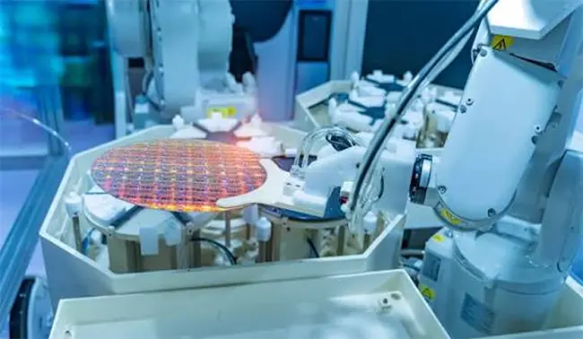

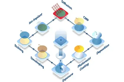
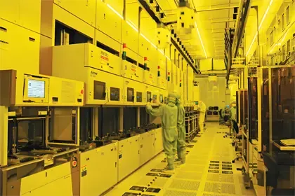
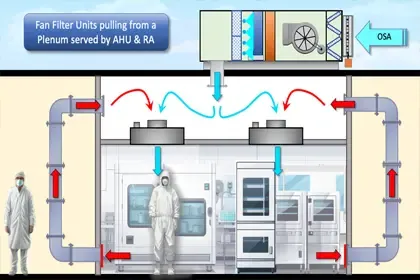
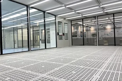


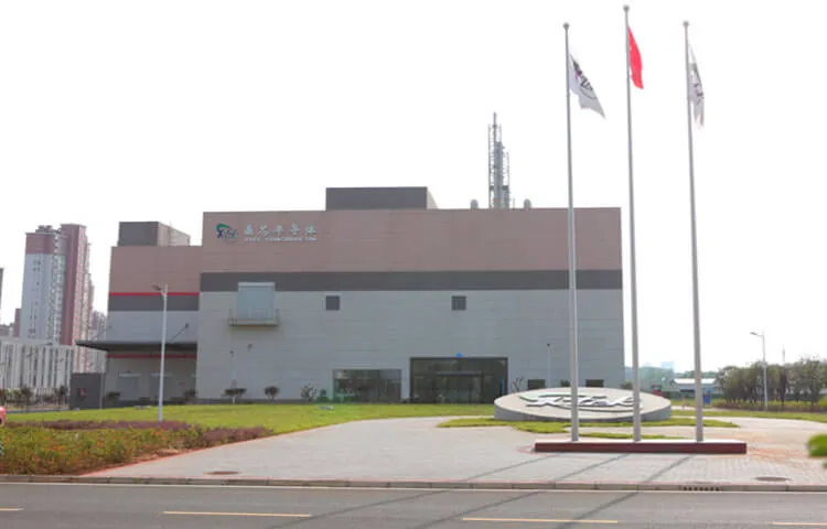
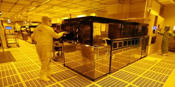
Design Review and Approval Ensure the design meets all required specifications. Site Preparation Prepare the location for installation, including structural supports and HVAC infrastructure. Cleanroom Structure Construction Install walls, ceilings, floors, and doors using the specified materials. HVAC and Filtration Systems Install HEPA/ULPA filters, air ducts, and ventilation systems to ensure proper airflow and contamination control. System Testing and Calibration Verify that all systems (temperature, humidity, airflow) are working as designed. Final Inspection and Certification Ensure compliance with international standards such as ISO 14644-1 before the cleanroom is operational.
Learn more about Deiiang cleanrooms

Brochure
Deiiang_Modular_Cleanroom_Solution_Proposal
■ Constructed on anodized extruded aluminum frame with sealed sandwich panel, HPL, acrylic or tempered-glass infill. ■ Suitable for ISO 5–8 per ISO 14644-1; positive or negative pressure cascade available. ■ Flush double-glazed observation windows, steel cleanroom doors with drop-down bottom seal. ■ Panels: rock-wool / glass-magnesium / paper-honeycomb / aluminum-honeycomb / PU core options. ■ HEPA H14 (EN 1822) as standard; ULPA U15/U16 option. ESD-safe conductive finish for electronics.
Brochure

Tech Resource
IEC 61340 5 1 2024.pdf
IEC 61340-5-1:2024 establishes the international requirements for an electrostatic discharge (ESD) control program, specifying the administrative and technical measures needed to protect sensitive electronic devices and assemblies from damage caused by electrostatic phenomena.
Tech Resource
SIST EN 1081 2019.pdf
SIST EN 1081:2019 specifies test methods for determining the electrical resistance of resilient floor coverings, including resistance to earth, vertical resistance, and resistance between points, to ensure effective static control in sensitive industrial and laboratory settings.
Tech Resource
European Standard 2024.pdf
EN 17242:2024 (the most significant European update for this period) establishes harmonized safety and performance requirements for recirculatory filtration fume cabinets (RFFCs), defining rigorous test methods for containment efficiency and filtration capacity to ensure the safe handling of hazardous chemicals in laboratories.
Tech Resource
IEC 61340 4 2010.pdf
IEC 61340-4:2010 is the 4th part of the IEC 61340 international electrostatics standard series, which specifies standardized test methods for specific electrostatic discharge (ESD) protection applications to validate the performance of static control products and protect sensitive electronic components from electrostatic damage in laboratory and manufacturing environments.
Tech Resource
Tech Resource
NFX_15-211_Brief.pdf
"Laboratory Ventilation – Ductless Fume Hoods – Part 1: Safety and Performance Requirements." Scope: Harmonized requirements in Europe for the safety, performance classification, testing, and marking of ductless fume hoods. This framework is being increasingly adopted across Europe.
Tech Resource
NFX_15-211_Brief.pdf
"Laboratory Fume Hoods – Ductless Filtered Fume Hoods – Classification, Performance, and Test Methods." Scope: Ductless fume hoods are classified according to filtration type (e.g., organic vapors, acids, formaldehyde). Test methods include airtightness, filtration efficiency, breakthrough time, and safety requirements. Widely used as a core technology reference by manufacturers in Europe and globally.
Tech Resource
Brochure
Deiiang Laboratory Furniture Equipment Product Catalog.pdf
Deiiang Laboratory Furniture Equipment Product Catalog is a comprehensive product reference document that details Deiiang’s full portfolio of professional laboratory furniture and equipment — including fume hoods, lab workbenches, chemical storage units and safety fixtures — with complete technical specifications and customizable solutions for scientific research, pharmaceutical, industrial testing and cleanroom laboratory applications.
Tech Resource
SIST EN 14175 3 2019.pdf
SIST EN 14175-3:2019 is the Slovenian national adoption of European standard EN 14175-3:2019, which specifies formal type test methodologies to verify the fume containment safety and operational performance of laboratory fume cupboards connected to dedicated exhaust air systems, as the testing complement to the mandatory performance requirements defined in EN 14175-2.
Tech Resource
EN 17242 2025.pdf
EN 17242:2025 is a European standard for recirculatory filtration fume cabinets (RFFCs) that specifies uniform design, manufacturing, type testing and on-site testing requirements, to ensure effective containment and filtration of hazardous airborne contaminants before exhaust air is recirculated back into the laboratory, and harmonizes safety performance benchmarks for filtered fume enclosures across Europe.
Tech Resource
EN 12792 2003.pdf
EN 12792:2003 is a European standard that defines unified terminology, measurement units, and graphical symbols for building ventilation and air-conditioning systems, providing a consistent lexical and visual reference for all ventilation-related European standards and engineering practices.
Tech Resource
ANSI ASSP Z9.5 2022.pdf
ANSI/ASSP Z9.5-2022 is an American National Standard focused on laboratory ventilation, which establishes minimum requirements and industry best practices for ventilation system design, fume hood performance testing, and formal Laboratory Ventilation Management Plans, to protect laboratory personnel from physical harm and overexposure to hazardous airborne contaminants.
Tech Resource
OSHA Lab Standard.pdf
The OSHA Laboratory Standard (29 CFR 1910.1450) is a U.S. federal occupational safety regulation that protects laboratory workers from health hazards caused by exposure to hazardous chemicals, by requiring laboratories to establish a written Chemical Hygiene Plan and implement corresponding safety training, exposure monitoring and risk control measures.
Tech Resource
SIST EN 16611 2023.pdf
SIST EN 16611:2023 (EN 16611:2023) specifies methods and test procedures for assessing the surface resistance of furniture to microscratching and evaluating surface durability. ([sis.se](https://www.sis.se/en/produkter/domestic-and-commercial-equipment-entertainment-sports/furniture/ss-en-166112023/?utm_source=openai))
White Paper